 TEKZARO
Computing
Intel surpasses one million High-NA EUV wafers processed, outpaces the rest of the industry combined — company also trailblazing giant 6×12 photomasks to speed production and lower costs
Intel Surpasses One Million High-NA EUV Wafers Processed, Outpaces Rest of Industry Combined
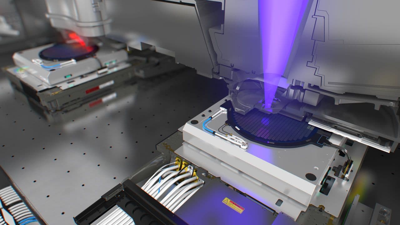
Intel announced at the SPIE Photomask Technology and Extreme Ultraviolet Lithography conference on September 8, 2026, that it has surpassed one million wafers processed using ASML's High-NA EUV lithography systems—a milestone that represents both extraordinary technological progress and Intel's commanding lead in next-generation semiconductor manufacturing. More significantly, Intel has processed more High-NA EUV wafers than the rest of the semiconductor industry combined, consolidating its position as the most experienced operator of this transformative technology.
The achievement marks the transition of High-NA EUV from experimental development tool to proven production technology. Intel is already using High-NA EUV on select layers of its Core Ultra Series 3 processors, code-named Panther Lake, which are based on the company's 18A (2nm-class) process technology. Performance, overlay accuracy, throughput, and availability are all meeting Intel Foundry's production expectations.
The Explosive Growth Trajectory
The pace of Intel's High-NA EUV adoption has accelerated dramatically. In late February 2025, Intel had processed approximately 30,000 wafers using High-NA EUV systems across tool certification, R&D, and early production work. Scaling from 30,000 wafers to over 1 million in approximately 18 months represents an explosive increase—roughly 33x growth in less than two years.
This acceleration demonstrates that Intel's High-NA production is moving beyond proof-of-concept into genuine high-volume manufacturing (HVM) territory. The company's two ASML Twinscan EXE:5000 tools and at least one EXE:5200B scanner are processing tens of thousands of wafers monthly—the kind of throughput required for commercial production at scale.
Production Today, Not Just Development
Critically, Intel's one million-wafer figure encompasses not just R&D and tool certification but actual volume production. The company is actively manufacturing chips using High-NA EUV technology for commercial processor lines. This distinguishes Intel's achievement from theoretical capability; Intel is proving that High-NA EUV can work reliably in production environments where yield, consistency, and throughput matter absolutely.
The fact that performance meets or exceeds comparable layers patterned using standard 0.33 NA EUV (conventional EUV) is particularly significant. It proves that High-NA EUV doesn't just work—it works as well as or better than the established technology it's meant to replace, with superior resolution enabling smaller transistor spacing.
The 6×12 Photomask Breakthrough
Alongside the one-million-wafer milestone, Intel is pioneering adoption of much larger photomasks. Current industry standard photomasks are 6 inches in diameter. Intel is trailblazing development and use of 6×12-inch photomasks—effectively doubling the mask size—which would allow High-NA EUV scanners to expose full 26×33 mm fields in a single pass without requiring field stitching.
This represents a fundamental architectural shift in semiconductor manufacturing. Current High-NA EUV systems can expose only 26×16.5 mm half-fields, which means large chips like GPUs and CPUs must be patterned using stitching—overlapping multiple exposures to cover the entire die. Stitching introduces complexity, alignment risks, overlay errors, and potential yield loss in the stitched regions.
The 6×12-inch mask would eliminate stitching entirely for most chip designs, immediately improving:
Throughput — Fewer exposure passes per layer means more wafers processed per unit time.
Yield — Eliminating stitch points removes sources of alignment defects and overlay error.
Design flexibility — Chip architects gain freedom to layout dies without worrying about stitching constraints.
Cost per wafer — Fewer exposures means lower per-wafer costs and better tool utilization.
However, implementing 6×12-inch masks requires transforming the entire semiconductor supply chain. Mask-inspection systems, reticle-handling equipment, and photomask-manufacturing infrastructure would all need redesign to accommodate masks four times larger than current standard sizes.
Intel's Strategic Position
Intel's lead in High-NA EUV processing represents a crucial competitive advantage heading into the AI chip manufacturing era. The company's early commitment to High-NA technology—while Samsung and TSMC waited—has translated into:
Technology leadership — More wafers processed means deeper understanding of how to optimize High-NA EUV manufacturing, troubleshoot issues, and maximize tool capability.
Supply chain influence — Intel's feedback shapes how ASML develops its High-NA scanners, giving Intel input into equipment roadmaps and potentially favorable access to new tools.
Photomask standardization — Intel's push for 6×12-inch masks positions the company as the standard-setter for next-generation mask infrastructure that will eventually become industry-wide.
First-mover advantage — Producing chips with High-NA EUV before competitors gives Intel experience with integration challenges that others will face years later.
The Equipment and Cost Barrier
Each ASML High-NA EUV system costs approximately $400 million—roughly double the price of standard 0.33 NA EUV machines. This extraordinary cost creates a substantial barrier to entry. Only the largest, most capital-rich manufacturers can afford to purchase multiple High-NA systems.
Intel's possession of at least three High-NA systems represents approximately $1.2 billion in equipment capital alone. Samsung and TSMC, while committing to High-NA adoption timelines of 2028 and 2030 respectively, have not yet deployed systems at scale. Intel has already deployed and amortized significant capital.
Additionally, High-NA EUV exposures cost approximately 2.5 times more than standard EUV exposures per wafer. This higher per-unit cost creates pressure to maximize tool utilization and minimize waste—another area where Intel's operating experience provides advantage.
Current Production Reality
Intel is using High-NA EUV for select layers of its 18A process technology on Panther Lake processors currently in production. This is not theoretical capability—it is proven technology delivering commercial processors to the market. The fact that performance meets or exceeds conventional EUV implementations validates that High-NA is production-ready.
Overlay accuracy, throughput, and tool availability all meet Intel Foundry's production requirements—meaning the technology is not just working but meeting commercial-grade expectations for precision, speed, and reliability.
What This Means for the Industry
Intel's one-million-wafer milestone and pioneering work with 6×12-inch masks signal several important implications for the semiconductor industry:
High-NA EUV is no longer experimental — With over a million wafers processed and active production underway, High-NA EUV has crossed from R&D curiosity to proven manufacturing technology.
Stitching limitations will be overcome — The industry has been concerned that stitching complexity could limit High-NA adoption. Intel's work on larger masks suggests a clear path to eliminate stitching constraints.
Intel has genuine foundry credibility — Intel's earlier technology gambles (High-NA EUV, aggressive process node roadmaps) are paying off with proven production capability that positions the company as a credible alternative to TSMC.
Supply chain must evolve — Adoption of 6×12-inch masks requires transforming mask-manufacturing and mask-inspection infrastructure globally—a multi-year, multi-billion-dollar ecosystem investment.
Competitive pressure increases — Samsung and TSMC must accelerate their High-NA timelines or risk falling further behind Intel in experience and capability.
The Path Forward
Intel's High-NA EUV leadership positions the company well as the semiconductor industry moves toward the 2033 roadmap outlined by ASML, TSMC, Samsung, and Intel. The company's production experience means Intel can troubleshoot issues, optimize processes, and maximize yield—advantages that will persist even after competitors deploy their own High-NA systems.
The 6×12-inch photomask development represents the next frontier. If Intel successfully proves larger masks work reliably in production, it will establish a new standard that other manufacturers must follow. This would give Intel disproportionate influence over how the industry standardizes High-NA technology for the remainder of this decade.
For now, Intel's achievement stands as a validation of the company's foundry strategy: invest in cutting-edge manufacturing technology ahead of competitors, develop expertise and supply-chain relationships, and leverage that advantage into competitive position. One million High-NA EUV wafers processed demonstrates that this strategy is working—at least on the technology front.
Sources
Related Articles