 TEKZARO
AI
ASML, TSMC, Samsung and Intel Agree on AI Chip Roadmap Through 2033
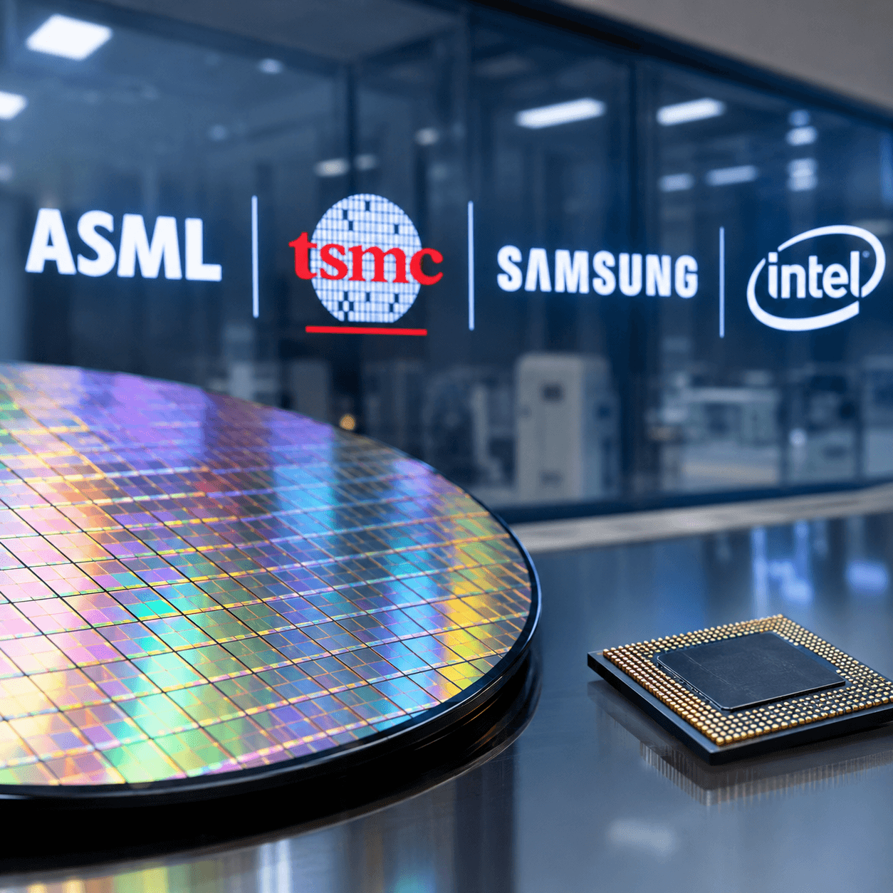
Four companies that collectively control nearly every advanced chip on Earth announced a coordinated technology roadmap on September 8, 2026, outlining how artificial intelligence processors will be manufactured for the next seven years. ASML, TSMC, Samsung, and Intel committed to a major infrastructure shift: transitioning from current 6-inch photomasks to a new 12-inch format paired with High-NA EUV lithography equipment costing approximately $400 million per machine.
The announcement represents an unprecedented alignment among the global semiconductor ecosystem's most critical players. By moving from 6-inch to 12-inch photomasks—quadrupling the template size that etches circuit patterns onto silicon wafers—the industry is betting on a fundamental manufacturing architecture change that will enable more powerful AI chips through 2033 and beyond.
The 12-Inch Photomask and High-NA EUV Strategy
The joint initiative centers on migrating to 12-inch photomasks paired with High-NA (High Numerical Aperture) EUV lithography systems. Current industry standard photomasks are 6 inches; the move to 12 inches represents a significant step in production capacity and precision.
High-NA EUV technology represents the cutting edge of semiconductor manufacturing capability, enabling the production of sub-3 nanometer circuitry with unprecedented precision. ASML manufactures these machines, and each system costs approximately $400 million—among the most expensive precision manufacturing equipment in the world.
The commitment to this specific technology path signals that ASML's High-NA approach has won industry consensus as the path forward for advanced AI chip production. This validation strengthens ASML's market position and justifies the massive R&D investment the company has made in High-NA technology development.
Timeline: Pilot Line by 2031, Production by 2033
The roadmap targets specific milestones:
Pilot Line by 2031: A 12-inch photomask pilot line will be established, allowing initial testing and development of manufacturing processes using the new mask format.
Production by 2033: Advanced-node production using 12-inch masks and High-NA EUV systems will begin, making the new technology commercially deployed.
This timeline allows approximately five years of development and optimization before commercial production scales. For comparison, major process technology transitions (like the industry's shift to EUV in 2017-2019) typically require multi-year pilot and refinement periods.
Adoption Timelines by Company
The roadmap specifies when each manufacturer will integrate ASML's High-NA EUV machines into high-volume production:
Samsung: 2028 — The Korean chipmaker will be first, adopting High-NA EUV machinery for DRAM and high-bandwidth memory (HBM) production. Samsung's entrance at 2028 gives the company a two-year head start before TSMC and positions Samsung to supply critical memory components for AI infrastructure.
TSMC: 2030 — Taiwan Semiconductor Manufacturing Company will adopt High-NA EUV for its foundry services, likely supporting custom AI chip production for Nvidia, Apple, AMD, and other leading-edge processor designers.
Intel: Already Deployed — Intel has already begun running wafers through High-NA EUV tools at scale, processing more than 1 million wafers according to Tom's Hardware reporting. The company also leads the industry in using larger 6x12 photomasks that the new 12-inch initiative depends on. Intel's head start reflects its earlier commitment to High-NA technology and positions the company as having the most production experience with this approach.
SK Hynix and Memory Infrastructure
SK Hynix, though not mentioned in the initial joint statement, represents a critical fourth pillar in AI chip manufacturing. The South Korean memory manufacturer placed an $8 billion order for EUV lithography tools in March 2026—the largest single disclosed order in company history—covering high-bandwidth memory and advanced DRAM production through 2027.
This $8 billion commitment ensures that HBM and DRAM capacity expands to meet the extraordinary demand for memory components in AI data centers. Memory serves as a critical constraint in AI system performance; without sufficient HBM and DRAM capacity, even the fastest processors face bandwidth bottlenecks.
Why This Matters: Solving the AI Bottleneck
The AI infrastructure buildout faces a critical capacity constraint: demand for advanced processors vastly exceeds manufacturing capacity. Current-generation AI chips require cutting-edge process nodes, which only TSMC, Samsung, and Intel (with Intel still proving its advanced foundry capabilities) can produce.
By committing to 12-inch photomasks and High-NA EUV through 2033, these four companies are essentially saying: "We're building the infrastructure to make enough AI chips for global demand through the end of this decade."
The commitment requires enormous capital investment. Each $400 million High-NA EUV machine represents a single-point expenditure that must be amortized through years of manufacturing. The coordinated commitment from multiple manufacturers provides confidence that orders will be stable enough to justify this investment.
Intel's Strategic Victory
Intel's advanced position in this roadmap represents a significant validation for the company's manufacturing transformation strategy. Under CEO Pat Gelsinger's leadership (and now continued under his successor), Intel has committed to becoming a foundry alternative to TSMC—a massive strategic pivot for a company historically focused on its own processor designs.
Intel's head start with High-NA EUV—already processing 1 million+ wafers compared to essentially zero for other players—suggests Intel's technology bet was correct and is paying strategic dividends. For Intel, becoming the first major manufacturer with High-NA production experience could translate into competitive advantage in the foundry market.
However, Intel's financial challenges have been severe, with the company requiring government subsidies through the CHIPS Act to fund its foundry buildout. The success of Intel's foundry business remains uncertain despite this technology leadership.
ASML's Monopoly Power
The agreement underscores ASML's dominant position in semiconductor equipment. There is effectively only one company globally that can manufacture High-NA EUV lithography systems: ASML. This monopoly status, while economically powerful, has also made ASML a geopolitical target.
The United States has imposed export controls preventing ASML from selling advanced lithography equipment to China, citing national security concerns. ASML has publicly acknowledged that this regulatory uncertainty affects investor confidence despite strong demand from non-China customers.
The multilateral agreement from TSMC, Samsung, and Intel represents validation that the three leading non-China chip manufacturers view ASML's High-NA path as essential infrastructure, regardless of geopolitical uncertainties.
Investment and Capital Requirements
Implementing this roadmap requires extraordinary capital investment across all four companies. Each manufacturer must fund:
- High-NA EUV machine purchases ($400M+ per unit, with multiple machines per facility)
- Facility construction and modification to accommodate new equipment
- Process development and optimization for 12-inch photomasks
- Workforce training and development
- Supply chain investments in mask production and supporting equipment
Industry analysts estimate the total capital expenditure required to implement this roadmap globally at tens of billions of dollars. For perspective, TSMC alone spent $36 billion on capital expenditures in 2025 and expects similar levels through 2027.
Competitive Implications
This agreement effectively locks in an equipment and technology pathway for the world's leading chip manufacturers through 2033. Companies that cannot afford or gain access to High-NA EUV technology will struggle to compete in advanced-node manufacturing.
This particularly affects:
Emerging manufacturers — Any startup or rising competitor would need to master High-NA technology to compete at leading nodes, requiring capital investment on a scale few new entrants could sustain.
Chinese manufacturers — Geopolitical restrictions prevent access to High-NA EUV tools, potentially widening the technology gap between Chinese and Western foundries.
Regional manufacturers — India, Japan, and other regions developing semiconductor capabilities must make strategic decisions about whether to chase leading-edge nodes (expensive, high-capital) or focus on trailing-edge and specialized production.
Timeline Context: Seven-Year Visibility
The seven-year visibility provided by this roadmap (2026 through 2033) is remarkably long for an industry where product cycles typically measure in years and technology transitions occur every 18-24 months.
This extended timeline reflects confidence that AI chip demand will remain robust through 2033, justifying multi-billion-dollar capital investments in equipment and infrastructure specifically optimized for AI processor manufacturing.
The roadmap essentially bets that artificial intelligence will remain a dominant demand driver for semiconductor manufacturing for at least seven more years—a remarkably long bullish statement on the AI industry's prospects.
What Comes Next
The immediate focus will be on Samsung's adoption of High-NA EUV by 2028. If Samsung successfully ramps memory production using these tools and delivers quality HBM and DRAM for AI data centers, it validates the technical approach and builds confidence for TSMC's subsequent 2030 transition.
TSMC's entry in 2030 will then drive High-NA adoption for custom AI chip manufacturing, potentially supporting new processor architectures and designs currently in development.
By 2031, when the 12-inch mask pilot line comes online, manufacturers will begin testing whether the larger mask format delivers expected benefits: improved throughput, better process control, and lower per-wafer costs that offset the $400 million machine investment.
Full production deployment by 2033 would make 12-inch High-NA the standard for advanced-node manufacturing, essentially retiring the current 6-inch photomask era entirely.
The Bottom Line
Four of the world's most critical technology companies just outlined the future of semiconductor manufacturing through 2033. The commitment to 12-inch photomasks, High-NA EUV equipment, and specific adoption timelines represents an unprecedented alignment on the technology roadmap that will enable AI chip production for the next seven years.
For investors, manufacturers, and AI companies dependent on leading-edge processors, this announcement provides clarity: the semiconductor industry is committing the capital, time, and resources necessary to manufacture AI chips at the scale and performance levels required for continued AI infrastructure expansion through 2033 and beyond.
Sources
Related Articles